Datasheet4U Logo Datasheet4U.com

74ACT11898 - 10-BIT PARALLEL-OUT SERIAL SHIFT REGISTER

General Description

The 74ACT11898

Key Features

  • AND-gated serial inputs and an asynchronous clear. The gated serial inputs (A and B) permit complete control over incoming data. A low at either input inhibits entry of new data and resets the first flip-flop to the low level on the rising edge of the next clock pulse. A high-level input enables the other input, which then determines the state of the first flip-flop. Data at the serial inputs may be changed while the clock is high or low provided the minimum setup and hold time requirements are.

📥 Download Datasheet

Full PDF Text Transcription (Reference)

The following content is an automatically extracted verbatim text from the original manufacturer datasheet and is provided for reference purposes only.

View original datasheet text
74ACT11898 10-BIT PARALLEL-OUT SERIAL SHIFT REGISTER • Inputs Are TTL-Voltage Compatible • AND-Gated (Enable/Disable) Serial Inputs • Fully Buffered Clock and Serial Inputs • Direct Clear • Fully Synchronous Data Transfers • Flow-Through Architecture Optimizes PCB Layout • Center-Pin VCC and GND Pin Configurations Minimize High-Speed Switching Noise • EPIC™ (Enhanced-Performance Implanted CMOS) 1-µm Process • 500-mA Typical Latch-Up Immunity at 125°C • Package Options Include Plastic Small-Outline Packages and Standard Plastic 300-mil DIPs SCAS144 – OCTOBER 1990 – REVISED APRIL 1993 
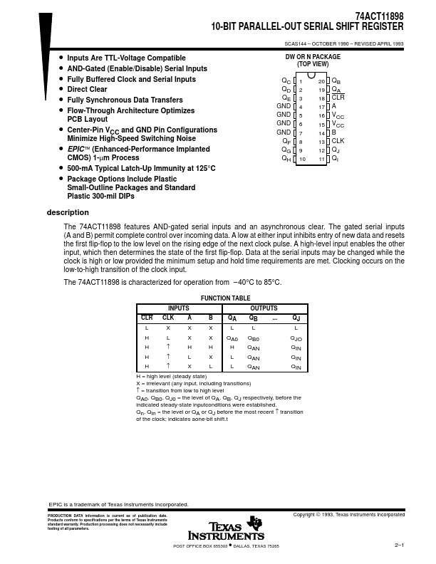
DW OR N PACKAGE (TOP VIEW) QC QD QE GND GND GND GND QF QG QH 1 2 3 4 5 6 7 8 9 10 20 QB 19 QA 18 CLR 17 A 16 VCC 15 VCC 14 B 13 CLK 12 QJ 11 QI description The 74ACT11898 features AND-gated serial inputs